Introduction
JTAG is an integrated method for testing interconnects on printed circuit boards (PCBs) that are implemented at the integrated circuit (IC) level. Since its introduction as an industry-standard in 1990, JTAG has continuously grown in adoption, popularity, and usefulness—even today, new revisions and supplements to the IEEE Std.-1149.1 standard are being developed and implemented. This document is a brief introduction to the nature and history of JTAG, from its introduction to new extensions in current development.
JTAG Technology
JTAG is commonly referred to as boundary-scan and defined by the Institute of Electrical and Electronics Engineers (IEEE) 1149.1, which originally began as an integrated method for testing interconnects on printed circuit boards (PCBs) implemented at the integrated circuit (IC) level. As PCBs grew in complexity and density—a trend that continues today—limitations in the traditional test methods of in-circuit testers (ICTs) and bed of nails fixtures became evident. Packaging formats, specifically Ball Grid Array (BGA, depicted in Figure 1) and other fine pitch components, designed to meet ever-increasing physical space constraints, also led to a loss of physical access to signals.
These new technology developments led to dramatic increases in costs related to designing and building a bed of nails fixtures; at the same time, circuit board test coverage also suffered. JTAG/boundary-scan presented an elegant solution to this problem: build functionality into the IC to assist in testing assembled electronic systems.
Today, JTAG is used for everything from testing interconnects and functionality on ICs to programming flash memory of systems deployed in the field and everything in-between. JTAG and its related standards have been and will continue to be extended to address additional challenges in electronic test and manufacturing, including a test of 3D ICs and complex, hierarchical systems.

History of JTAG
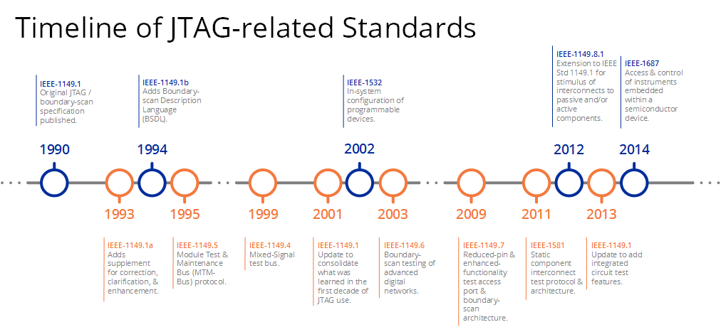
In the 1980s, the Joint Test Action Group (JTAG) set out to develop a specification for boundary-scan testing that was standardized in 1990 as the IEEE Std. 1149.1-1990. A few years later in 1993, a new revision to the standard—1149.1a—was introduced to clarify, correct, and enhance the original specification. An additional supplement, 1149.1b, was published in 1994 to add Boundary-Scan Description Language (BSDL) to the standard, paving the way for fast, automated test development and spurring continuous adoption by major electronics producers all over the world. The lessons that were learned became formalized in an update to the core standard in 2001 and IEEE-1149.1-2001 was published.
As new applications of JTAG were discovered, new standards were developed to extend the capabilities of JTAG. Standards such as the IEEE-1149.5 module test and maintenance bus standard in 1995 and the IEEE-1149.4 standard for mixed-signal testing in 1999 were met with low adoption rates and are not widely used at present. The IEEE-1149.6 standard introduced in 2003, on the other hand, began with slow adoption but has since become standard in many ICs as the technology it addressed—high-speed, AC-coupled signals—became a common feature of electronic systems. IEEE-1149.7, published in 2009 to address the need for JTAG in low-pin-count systems, is now standard on many popular microcontrollers.
What is JTAG?
Additional standards have also been published to add specific test capabilities. In 2002, the IEEE-1532 standard for in-system configuration of programmable devices was released and is now a common feature of FPGAs and their supporting software systems. IEEE-1581 was developed in 2011 to provide a convenient method of testing interconnects of high-speed memories with slow-speed test vectors; a version of this capability is implemented in some DDR4 memory components. To address the new application of combined capacitive sensing and boundary-scan test, IEEE-1149.8.1 was published in 2012. The extensibility of JTAG has been proven time and again.
More recently, efforts have been made to standardize JTAG access to instruments embedded within ICs. The IEEE-1149.1 standard was updated once more in 2013 for some housekeeping and to add extensions to access these instruments. Just one year later, an alternative standard for accessing these instruments, IEEE-1687, was published. Looking to the future, industry activities to extend JTAG into 3D-IC testing, system-level testing, and high-speed testing are already underway, proving that the versatility and extensibility of JTAG are here to stay.
Here’s the video for understanding easily – https://www.youtube.com/watch?v=uQs32JjZrhs
How Does JTAG Work?
The JTAG/boundary-scan test architecture was originally developed as a method to test interconnects between ICs mounted on a PCB without using physical test probes. Boundary-scan cells created using multiplexer and latch circuits are attached to each pin on the device. These cells, embedded in the device, can capture data from pin or core logic signals as well as force data onto pins. Captured data is serially shifted out through the JTAG Test Access Port (TAP) and can be compared to expected values to determine a pass or fail result. Forced test data is serially shifted into the boundary-scan cells. All of this is controlled from a serial data path called the scan path or scan chain.
Because each pin can be individually controlled, boundary-scan eliminates a large number of test vectors that would normally need to properly initialize sequential logic. Using JTAG, tens or hundreds of test vectors may do the job that had previously required thousands. Boundary-scan enables shorter test times, higher test coverage, increased diagnostic capability, and lower capital equipment cost.
Corporate Headquarters
Corelis, Inc.
13100 Alondra Blvd. Suite 102
Cerritos, CA 90703
Sales & General Inquiries
Toll-Free: 888.808.2380
Fax: 562.404.6196
Email: sales@corelis.com


No Comments